Résumé
As optical communication modules and precision electronics require higher thermal stability, Puce TEC reliability under repeated thermal cycling has become a critical factor in system performance and product qualification.
This article explores the key causes of TEC chip degradation, including solder fatigue, material interface failure, and thermal expansion mismatch, while explaining reliability standards such as Telcordia GR-468 and AEC-Q100. It also examines how advanced technologies enable million-cycle endurance and provides practical guidance for engineers and procurement managers selecting high-reliability thermoelectric cooler chips for optical modules, laser systems, and precision cooling applications.
1. What Makes a TEC Chip Fail Under Repeated Thermal Cycling
1.1 Root Causes of Performance Degradation in Thermoelectric Cooler Chips
TEC chip failure under cyclic thermal stress is rarely a sudden event. It is a progressive accumulation of micro-damage across three primary mechanisms.
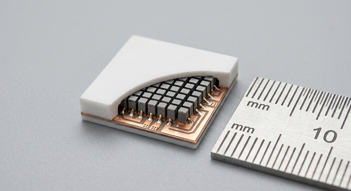
Solder joint fatigue is the dominant failure mode. Each thermal cycle generates mechanical strain at the interface between the thermoelectric element and the copper electrode, driven by differential thermal expansion. Over tens of thousands of cycles, this initiates micro-cracks that propagate until electrical continuity is compromised—manifesting as rising internal resistance and declining cooling capacity.
Bi₂Te₃ interface degradation is equally critical. Bismuth telluride, the standard thermoelectric semiconductor in commercial TEC chips, is inherently brittle. Repeated thermal excursions cause grain boundary sliding and interdiffusion at the metal-semiconductor interface, degrading the Seebeck coefficient and increasing thermal conductivity—both of which reduce the effective ΔTmax the chip can sustain.
CTE mismatch cumulative damage compounds both mechanisms. When the coefficient of thermal expansion (CTE) of the ceramic substrate, solder layer, and Bi₂Te₃ element are not closely matched, each cycle deposits residual stress. Over time, this stress concentration—particularly at substrate corners and element edges—accelerates delamination and fracture.
1.2 Material and Structural Factors That Accelerate Failure
Beyond intrinsic material properties, design and process choices significantly influence cycle life. Choix du matériau du substrat is foundational: Al₂O₃ substrates offer cost efficiency but exhibit higher CTE values (~7 ppm/°C) compared to AlN (~4.5 ppm/°C), making AlN the preferred choice in high-cycle applications where CTE matching to Bi₂Te₃ (~16 ppm/°C) must be managed through intermediate bonding layers.
Electrode oxidation at copper metallization surfaces introduces contact resistance that compounds with each thermal cycle. Without protective surface treatments or hermetic packaging, oxidation-driven resistance drift can account for 30–50% of total ΔR/R over a chip’s service life.
Packaging stress concentration at element-to-substrate bonds is often underestimated. Poorly controlled solder void fractions—above 5% by area—create thermal hotspots that locally accelerate fatigue, reducing effective cycle life by an order of magnitude relative to void-free bonds.
2. Engineering Standards and Test Protocols for TEC Chip Reliability
2.1 Industry Benchmarks: What “1,000,000 Cycles” Actually Means
The figure “1,000,000 thermal cycles” is meaningful only when tied to a defined test protocol. Three standards dominate high-reliability TEC chip qualification:
Telcordia GR-468 is the primary reference for optical component reliability. It specifies thermal cycling between −40°C and +85°C at a ramp rate of ≤10°C/minute, with dwell times of ≥10 minutes at each extreme. Passing criteria typically require ΔR/R < 10% and no catastrophic opens or shorts after the specified cycle count. For telecom-grade TEC chips, GR-468 compliance is effectively mandatory.
AEC-Q100 (Grade 1 and Grade 0) applies to automotive-grade thermoelectric cooler chips, specifying cycling from −40°C to +125°C or +150°C, respectively. The higher temperature ceiling and faster ramp rates (up to 15°C/minute) make AEC-Q100 qualification a more severe stress screen than GR-468—chips that pass AEC-Q100 Grade 0 typically demonstrate superior margin in telecom environments.
MIL-STD-883 Method 1010 governs military and aerospace applications, with cycle ranges extending to −65°C/+150°C and pass/fail criteria defined by visual inspection and electrical parametric limits.
2.2 Key Performance Metrics Measured Across the Cycle Life
Three parameters serve as the quantitative backbone of TEC chip reliability assessment:
- ΔTmax degradation rate: The percentage reduction in maximum achievable temperature differential from the initial value. Industry consensus for optical module applications holds ΔTmax degradation to ≤5% after 500,000 cycles as the acceptance threshold.
- Resistance drift (ΔR/R): Internal resistance increase expressed as a percentage of initial value. Values exceeding 10% typically indicate solder joint or electrode degradation sufficient to impact system-level thermal performance.
- COP trend: Coefficient of performance decline across cycle life reflects combined degradation of thermoelectric efficiency and thermal conductance. COP monitoring enables early detection of Bi₂Te₃ interface degradation before catastrophic failure.
| Paramètre | Typical Threshold | Test Standard | Measurement Interval |
|---|---|---|---|
| Thermal Cycles | 100K / 500K / 1M | GR-468 / AEC-Q100 | Every 100K cycles |
| ΔTmax Degradation | ≤5% at 500K cycles | GR-468 | Pre/post + interim |
| ΔR/R Resistance Drift | <10% at test end | GR-468 / MIL-STD | Every 100K cycles |
| Operating Temp Range | −40°C to +85°C / +125°C | Per application grade | Full range sweep |
| Substrate Material | AlN preferred over Al₂O₃ | Design spec | N/A |
| Solder Void Fraction | <5% by X-ray | Internal QC | Per lot |
| Applications typiques | Optical modules, LiDAR, laser temp control | Application-specific | N/A |
3. Design Innovations That Enable Million-Cycle Endurance
3.1 Advanced Bonding and Substrate Technologies in High-Reliability TEC Chips
Achieving 1,000,000-cycle endurance requires deliberate engineering at every material interface. Three innovations have demonstrated measurable impact:
Direct Bonded Copper (DBC) substrate technology replaces conventional brazing with a direct oxide-bonded copper-ceramic interface, eliminating the intermediate bonding layer that is a common fatigue initiation site. DBC on AlN substrates achieves thermal conductivity >170 W/m·K while maintaining CTE compatibility with Bi₂Te₃ elements—critical for minimizing differential strain per cycle.
AuSn solder replacing SAC alloys at the element-to-substrate bond is a high-impact reliability upgrade. AuSn (80/20) exhibits a melting point of 280°C and superior creep resistance compared to standard SAC305 alloys, which soften above 100°C under cyclic loading. In accelerated life testing, AuSn-bonded TEC chips demonstrate 3–5× longer fatigue life than SAC-bonded equivalents under identical cycling conditions.
Nanoscale Bi₂Te₃ grain homogenization through controlled powder metallurgy and hot-press sintering reduces grain boundary density and improves mechanical isotropy. Uniform microstructure suppresses preferential crack propagation paths, directly extending the cycle life of the thermoelectric element itself.
3.2 Miniaturization Trends and Their Impact on Thermal Cycling Performance
The push toward sub-3×3 mm TEC chips for compact optical transceivers introduces competing constraints: reduced element cross-section increases current density and localized heat flux, while smaller substrate area reduces the thermal mass available to buffer transient temperature excursions.
High-cycle miniaturized TEC chips address this through optimized element aspect ratio control—taller, narrower Bi₂Te₃ pillars reduce lateral CTE-induced strain while maintaining ΔTmax. Precision dicing and element placement tolerances below ±10 µm minimize parasitic thermal resistance at element edges, which is disproportionately impactful at small scales. Combined with DBC substrates and AuSn bonding, miniaturized TEC chips rated to ≤3×3 mm can achieve million-cycle performance equivalent to full-size modules—provided the thermal interface to the system heat spreader is engineered with equal rigor.
4. Application Scenarios and Commercial Value for B2B Buyers
4.1 Critical Use Cases: Optical Communication, Laser Modules, and Precision Electronics Cooling
100G/400G optical transceivers represent the highest-volume application for high-reliability TEC chips. A single 400G QSFP-DD module may accumulate 500,000+ thermal cycles over a 10-year deployment in a data center with daily temperature swings—making GR-468-qualified chips the only defensible specification. ΔTmax stability directly governs wavelength drift in DWDM systems; a 1°C temperature error at the laser junction translates to ~12 pm wavelength shift, sufficient to cause channel crosstalk.
DFB laser temperature stabilization demands ΔTmax degradation below 3% over service life. Even marginal cooling capacity loss forces the laser drive current higher to compensate, accelerating laser aging and ultimately shortening system MTBF.
LIDAR detector cooling in automotive and industrial applications combines AEC-Q100 thermal cycling requirements with vibration exposure, making AuSn-bonded, AlN-substrate TEC chips the engineering standard for programs targeting 150,000+ vehicle operating hours.
4.2 Total Cost of Ownership: Reliability as a Procurement Decision Factor
The price delta between a standard TEC chip and a million-cycle-qualified component is typically 15–40%. The TCO calculation, however, consistently favors the higher-reliability part:
- MTBF impact: A TEC chip with 2× the cycle life in a system running 24/7 can extend mean time between failures from 5 years to 10+ years—reducing field service events that cost $500–$2,000 per incident in telecom infrastructure.
- Warranty liability reduction: For module OEMs, specifying GR-468-compliant TEC chips shifts reliability risk to a quantified, tested parameter rather than an estimated one—directly reducing warranty reserve requirements.
- Supply chain risk: Suppliers capable of providing standardized test reports (GR-468, AEC-Q100) with lot traceability reduce qualification risk for new product introductions, compressing time-to-market by 4–8 weeks compared to sourcing from unqualified vendors.
FAQ
Q1: How do I verify a TEC chip supplier’s claim of 1,000,000 thermal cycle endurance—what test reports and standards should I request?
Request the full Telcordia GR-468 or AEC-Q100 qualification test report, including raw data for ΔR/R and ΔTmax at each measurement interval, the specific temperature profile used (ramp rate, dwell time, temperature range), sample size (minimum 22 units per GR-468), and lot traceability linking the tested samples to production lots. Third-party laboratory certification adds significant credibility. Reject any supplier that provides only a summary pass/fail statement without underlying parametric data.
Q2: What is the acceptable ΔTmax degradation rate after 500,000 cycles for optical communication module applications?
The industry-accepted threshold for telecom optical modules is ≤5% ΔTmax degradation at 500,000 cycles under GR-468 conditions (−40°C to +85°C). For DWDM applications with tight wavelength budgets, some system architects specify ≤3% to maintain a wavelength stability margin across the full product life. Confirm which threshold applies to your link budget before finalizing the TEC chip specification.
Q3: Does miniaturizing a TEC chip inherently compromise its thermal cycling reliability, or can it be engineered to match full-size module performance?
Miniaturization introduces higher current density and reduced thermal mass, which are reliability challenges—but they are engineering problems, not fundamental limits. TEC chips at ≤3×3 mm using AlN DBC substrates, AuSn bonding, and optimized element aspect ratios have demonstrated million-cycle performance in qualification testing. The key is verifying that the supplier has specifically qualified the miniaturized geometry, not extrapolating from larger module data.
FAQ
Million-cycle thermal cycling reliability is now a key requirement for TEC chips used in optical communication, laser temperature control, and precision cooling systems. With failure mechanisms such as solder fatigue, Bi₂Te₃ interface degradation, and CTE mismatch clearly identified, manufacturers can improve long-term performance through advanced solutions including AlN DBC substrates, AuSn bonding, and optimized thermoelectric element structures.
For engineers and procurement teams, selecting a reliable TEC chip requires more than reviewing datasheets. Verified reliability testing, thermal cycling data, material traceability, and supplier qualification capabilities are essential evaluation criteria. Although million-cycle-qualified thermoelectric cooler chips may require a higher initial investment, their improved durability can reduce maintenance costs, extend system lifetime, and lower total ownership costs. In mission-critical thermal management applications, reliability is not an added advantage—it is the foundation of long-term performance.